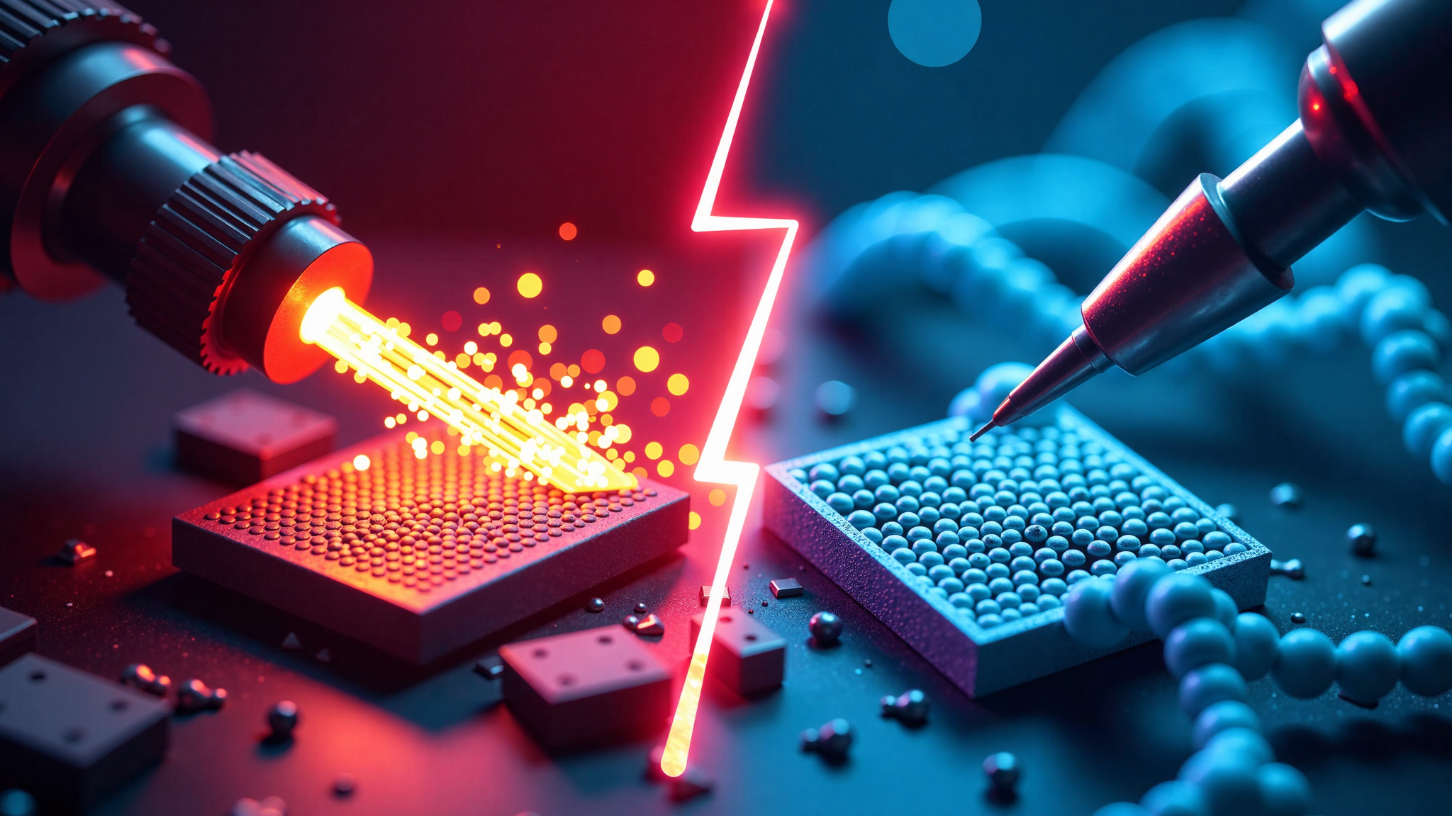
AFM vs. SEM: Choosing the Right Microscope for Nanoscale Success
The ability to explore the microscopic world has been rapidly growing with the recent development of new technologies such as nanotechnology, microbiology, and electronics. Since a microscope is a tool that provides magnified images of smaller objects, much research has been done on developing different microscopy techniques to increase resolution. While the first microscopes were optical solutions using lenses to magnify images, current high-resolution microscopes follow different approaches. Atomic Force Microscopy (AFM) and Scanning Electron Microscopy (SEM) are two such techniques with different approaches. Choosing between Atomic Force Microscopy (AFM) and Scanning Electron Microscopy (SEM) depends on your specific research needs, sample characteristics, and the type of information you seek to obtain.
What is SEM?
Scanning Electron Microscopy (SEM) utilizes a focused beam of electrons to scan the surface of a sample, producing detailed images of surface morphology. When the electron beam interacts with the sample, it generates secondary electrons, backscattered electrons, and characteristic X-rays, which are detected to form an image or provide compositional information. SEM excels in providing detailed images of surface structures with high lateral resolution (1-10 nanometers). SEM can be combined with techniques like Energy Dispersive X-ray Spectroscopy (EDS) for elemental analysis.
SEM is particularly well-suited for analyzing surface morphology, especially in conductive materials and bulk samples. It is widely used in fields like materials science and metallurgy. SEM images give an idea of the shape and dimensions of sample features. Other detectors produce contrast based on the atomic number. One of the most useful techniques is EDX, which can measure the types of elements present and even give concentrations of different elements. With EDX mapping, the distribution of different elements over an area can be displayed.
One of the key advantages of the SEM with respect to other types of microscopy is its large depth of field. This ability makes it possible to image very rough surfaces with millimeters of vertical information within a single image. The depth of field and small beam size make it possible to image the fibers far below the top layer. It also makes it possible to measure very rough surfaces over larger lateral areas.
What is AFM?
Atomic Force Microscopy (AFM) employs a sharp tip attached to a cantilever that scans the surface of a sample. As the probe moves, it interacts with the surface forces, and these interactions are measured to create high-resolution images. AFM excels in providing true 3D surface profiles and is capable of imaging soft materials and biological samples in their natural states. It’s also adept at measuring nanomechanical properties, such as elasticity and adhesion. AFM provides magnification in x, y, and z dimensions. An AFM picture allows users to quantify the height of a sample feature directly, whereas a SEM sample often requires cross-sectioning.
AFM can operate in various environments, including air, vacuum, liquids, and controlled atmospheres, allowing the study of samples in their natural or near-natural states. This versatility is particularly valuable for studying samples that require hydration, such as biological materials, or that are sensitive to oxygen or humidity. AFM typically requires minimal sample preparation and preserves the sample’s native state. AFM also offers multiple operation modes to characterize local sample properties such as conductivity, surface potential, and stiffness. Although the AFM can measure vertical surface variations below 0.5Å, its ability to measure a tall structure comes from how far the scanner can move vertically. Standard scanners typically have 5 to 6µm of vertical range.
AFM vs SEM
| Feature | AFM (Atomic Force Microscopy) | SEM (Scanning Electron Microscopy) |
|---|---|---|
| Resolution | Higher, capable of atomic-scale resolution | High, limited by electron interactions |
| Sample Type | Suitable for almost any sample, including soft and biological materials | Best for conductive, coated non-conductive samples |
| Surface Interaction | Direct contact or near-field forces between probe and sample | No direct contact; utilizes electron beam-sample interactions |
| 3D Imaging | Provides true 3D surface mapping | Limited depth perception |
| Imaging Speed | Slower but offers more detailed information | Faster imaging |
| Vacuum Requirement | No vacuum needed; can operate in ambient conditions | Requires a vacuum environment |
| Sample Preparation | AFM typically requires minimal sample preparation and preserves the sample’s native state | SEM samples must be carefully fixed and dried in sequential solutions |
| Information | Height, magnetism, and friction | Shape and dimensions of surface features |
How to Choose
Researchers should carefully evaluate their specific needs, sample characteristics, and research goals to select the most appropriate nanoscale imaging technique.
- Start with Your Question: What information are you trying to obtain from your sample? Are you looking for surface topography, material identification, or mechanical properties?
- SEM for Speed and Morphology: Choose SEM if you need fast imaging and detailed surface morphology of conductive/hard materials or samples with rough surfaces and significant vertical variations. SEM is ideal when a broad overview and high throughput are needed.
- Example: Analyzing the fracture surface of a metal component.
- AFM for Nanoscale Detail and Force Measurement: Choose AFM if you need atomic-level resolution, precise 3D surface profiles, and force measurements (elasticity, adhesion) or if you’re working with soft/non-conductive materials. Also, if you need to image in liquid or gas conditions to maintain sample integrity.
- Example: Characterizing the surface roughness of a thin film or imaging biological molecules in their native environment.
- The Sample Environment Matters:
- Vacuum Compatibility: SEM requires a vacuum environment, potentially altering or damaging delicate samples.
- Environmental Control: AFM allows imaging in ambient air, liquid, or controlled atmospheres, crucial for studying dynamic processes or hydrated samples.
- Consider a Combined Approach: Sometimes, the best solution is to use both techniques. Combining both techniques provides a more comprehensive analysis, where SEM gives a broad overview, and AFM zooms in for detailed nanoscale characterization.
- Example: Use SEM to identify a region of interest on a microdevice, then use AFM to analyze its surface roughness and mechanical properties.
- Budget and Expertise: SEM often involves higher upfront costs and more complex sample preparation. AFM can be more accessible, but interpreting data and minimizing artifacts requires expertise.
Enhance Your Understanding with Our YouTube Video
To further illustrate the concepts discussed in this article, we’ve created a detailed YouTube video that provides visual examples and practical demonstrations of AFM and SEM techniques.
- Visual Learning: See real microscope footage and animations that explain how each technique works.
- Practical Tips: Get insights into sample preparation, image analysis, and troubleshooting.
- Expert Insights: Hear directly from experts in the field about the best applications for each microscopy method.
Check out the video below to deepen your understanding and see these powerful tools in action!
Don’t forget to like, subscribe, and share to help us bring more educational content to the scientific community.
Conclusion
Both SEM and AFM are powerful microscopy techniques, each with its unique advantages. Your choice should align with your specific application requirements, sample characteristics, and the type of information you seek to obtain. By understanding the strengths and limitations of each technique, researchers can make informed decisions to achieve their desired results. Leveraging platforms like YouTube can further enhance understanding and accessibility to these powerful tools.
Check articles on https://inscilab.tech/category/general/ , https://inscilab.tech/category/sem/ , https://inscilab.tech/category/afm/ , https://inscilab.tech/category/xrd/
If the above doesn’t work, click here.