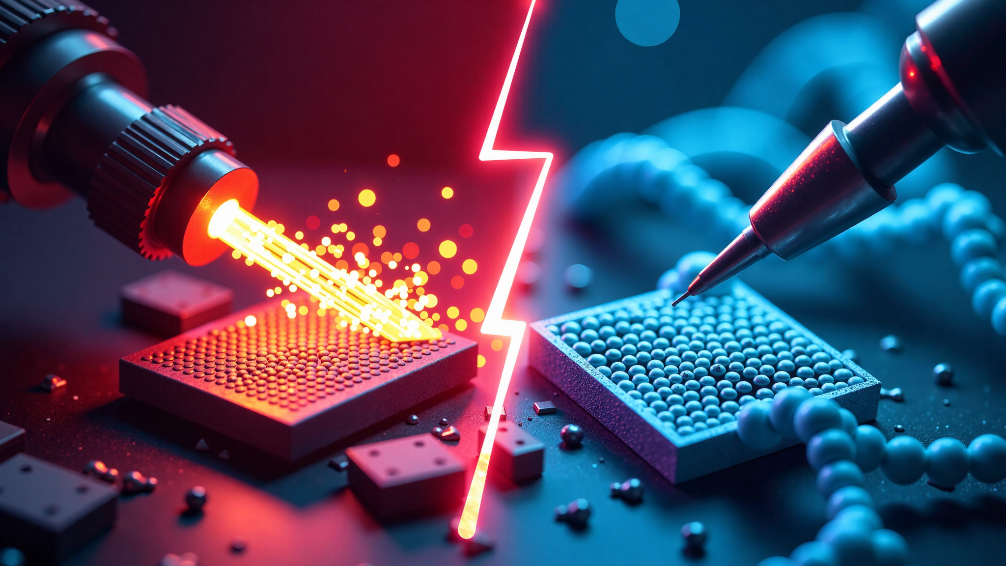
AFM vs SEM: How to Choose the Right Microscopy Technique
AFM vs SEM: The Definitive Guide to Nanoscale Imaging Selection
Struggling to choose between AFM and SEM for your research? This definitive guide compares their resolution limits, sample requirements, and applications to help you select the perfect technique for materials science, biology, or nanotechnology.
Table of Contents
Choosing between Scanning Electron Microscopy (SEM) and Atomic Force Microscopy (AFM) is a critical first step in any nanoscale investigation. The SEM vs AFM decision hinges on a fundamental trade-off: Do you need the rapid, high-resolution imaging of surface morphology that SEM provides, or the detailed 3D topography and nanomechanical property mapping unique to AFM? Selecting the wrong tool can cost you precious time, compromise delicate samples, or yield incomplete data. This guide cuts through the complexity, providing a clear, actionable framework to determine the ideal technique for your specific application in materials science, biology, or nanotechnology.
✅ Choose SEM For:
- Fast, high-resolution imaging of conductive or coated samples
- Exceptional depth of field for analyzing rough surfaces
- Elemental composition analysis (EDS)
- Broad overview and rapid screening of sample morphology
- High-throughput automated imaging for multiple samples
✅ Choose AFM For:
- True 3D surface topography with atomic-level resolution
- Measurement of nanomechanical properties (elasticity, adhesion)
- Imaging of soft, biological, or non-conductive materials
- Operation in liquid environments or ambient conditions
- Minimal sample preparation
What is Scanning Electron Microscopy (SEM)?
Scanning Electron Microscopy (SEM) is a powerful surface imaging technique that uses a focused beam of high-energy electrons to generate detailed, top-down images of a sample’s surface. Unlike optical microscopes, SEM can achieve remarkable lateral resolution down to 1-10 nanometers, revealing features invisible to light-based systems.
How SEM Works: A Quick Overview
- Electron Beam Generation: A beam of electrons is produced and focused onto the sample surface.
- Sample Interaction: The electrons interact with the atoms in the sample, generating various signals.
- Signal Detection: These signals—including secondary electrons (for surface topography) and backscattered electrons (for compositional contrast)—are collected by detectors.
- Image Formation: The signals are translated into a high-resolution, black-and-white image of the surface.
Key Strengths and Applications
- Exceptional Depth of Field: SEM’s large depth of field allows it to keep rough, uneven surfaces in sharp focus across a wide area, making it ideal for examining fracture surfaces, powders, and textured coatings.
- Elemental Analysis with EDS/EDX: When coupled with Energy Dispersive X-ray Spectroscopy (EDS or EDX), SEM can identify the elemental composition of the sample and even create maps showing the spatial distribution of elements.
- High-Throughput Imaging: SEM is relatively fast, making it excellent for screening large sample areas or multiple samples quickly to identify regions of interest.
Ideal Use Cases for SEM
- Analyzing the fracture surface of a metal alloy to determine failure mode.
- Characterizing the morphology and size distribution of nanoparticles or fibers.
- Inspecting the topography of integrated circuits and microelectronic devices.
- Performing elemental contamination analysis on a filter or surface.
Key Consideration: SEM typically requires samples to be electrically conductive. Non-conductive materials must be sputter-coated with a thin metal layer (like gold or platinum) to prevent charging and ensure a clear image.
What is Atomic Force Microscopy (AFM)?
Atomic Force Microscopy (AFM) is a high-resolution scanning probe technique that creates 3D images by physically feeling the surface with a sharp tip. Unlike SEM, AFM does not use lenses or electron beams, but instead relies on mechanical probing to achieve sub-nanometer resolution, making it capable of resolving atomic-scale features.
How AFM Works: The Core Principle
An AFM uses a sharp tip on a flexible cantilever as a physical probe. As this tip scans the sample surface, subtle atomic forces between the tip and the surface cause the cantilever to deflect. A laser beam reflected off the cantilever tracks these deflections with extreme precision, building a detailed, 3D topographical map of the surface.
Key Strengths and Applications
- True 3D Topography: AFM provides direct, quantitative height information, allowing for precise measurement of surface roughness, step heights, and particle size without the need for cross-sectioning.
- Nanomechanical Property Mapping: Beyond imaging, AFM can measure local properties such as elasticity (modulus), adhesion, and stiffness through force spectroscopy.
- Versatile Imaging Environments: AFM can operate in ambient air, controlled atmospheres, liquid, or vacuum. This makes it ideal for studying biological samples in physiological buffers, dynamic chemical processes, or air-sensitive materials.
- Minimal Sample Preparation: Most samples require little to no preparation and do not need to be conductive, preserving them in their native state.
Ideal Use Cases for AFM
- Measuring the true 3D surface roughness of a thin film or optical coating.
- Imaging live cells or proteins in their natural, hydrated state.
- Characterizing the mechanical properties of a polymer blend at the nanoscale.
- Profiling the depth and shape of nano-patterns on a semiconductor wafer.
Key Consideration: AFM has a relatively small maximum scan size (typically up to ~100µm) and a limited vertical range (~5-6µm for standard scanners). It is also a slower imaging technique compared to SEM, making it less suitable for high-throughput screening of large areas.
AFM vs SEM: Head-to-Head Technical Comparison
The AFM vs SEM table below provides a direct, side-by-side comparison of the core technical specifications and capabilities of AFM and SEM to help you make a data-driven choice.
| Feature | AFM (Atomic Force Microscopy) | SEM (Scanning Electron Microscopy) |
|---|---|---|
| Fundamental Principle | Mechanical probing of surface forces | Electron beam-sample interactions |
| Best Resolution | Suitable for almost any sample, Sub-nanometer (atomic-scale in some cases) | 1-10 nm (lateral) |
| 3D Capability | True 3D topography with quantitative height data | Pseudo-3D; limited depth perception |
| Sample Environment | Air, liquid, vacuum, controlled atmospheres | High vacuum (typically) |
| Sample Types | Excellent for soft, biological, & non-conductive materials | Best for conductive, solid samples; non-conductives require coating |
| Sample Preparation | Minimal (often none required) | Extensive (fixing, drying, conductive coating) |
| Imaging Speed | Slow (seconds to minutes per image) | Fast (seconds per image) |
| Depth of Field | Low | Exceptionally high |
| Primary Data | Surface height, nanomechanical properties (elasticity, adhesion) | Surface morphology, elemental composition (with EDS) |
| Maximum Scan Size | ~100 µm x 100 µm (typical) | Millimeters (large area mapping) |
JEOL’s SEM technical specifications | Park System’s AFM Specifications
Key Takeaways from the Comparison:
- For True 3D & Mechanical Properties: AFM is the undisputed choice when you need quantitative height measurements or data on material properties like stiffness and adhesion at the nanoscale.
- For Speed & Overview: SEM is superior for quickly imaging large areas, examining rough surfaces thanks to its high depth of field, and when elemental analysis (EDS) is required.
- The Sample is Key: The nature of your sample often dictates the choice. AFM for delicate, soft, or liquid-based samples; SEM for robust, conductive, or coated samples that can withstand a vacuum.
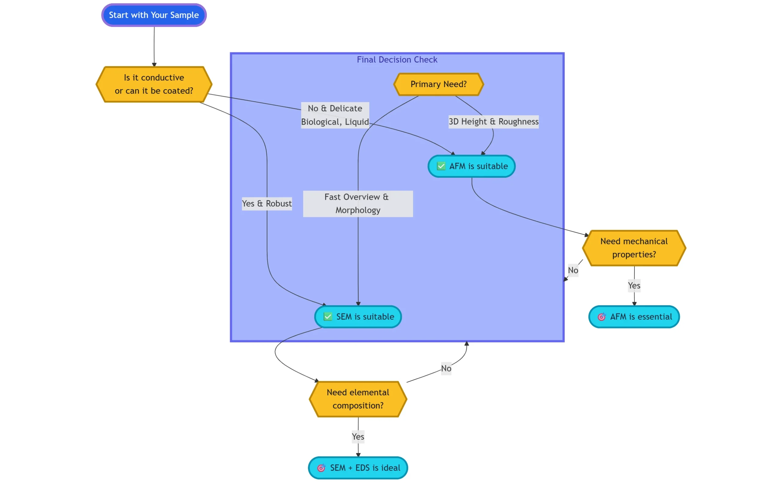
How to Choose: Your Decision-Making Framework
Selecting AFM vs SEM doesn’t need to be complex. Follow this structured approach to confidently determine the right technique for your research.
Step 1: Define Your Primary Goal
Start by asking the most critical question: What is the single most important piece of information I need?
- Choose AFM if your answer is: “True 3D surface topography,” “Nanomechanical properties (elasticity, adhesion),” or “To see the sample in its native, hydrated state.”
- Choose SEM if your answer is: “Rapid surface morphology overview,” “Elemental composition,” or “To image a large or very rough surface area.”
Step 2: Evaluate Your Sample
Your sample’s characteristics often make the decision for you. Use this flowchart to guide you:
Step 3: Decision Scenarios in Practice
When SEM is the Clear Winner:
- Scenario: You need to identify the cause of failure in a steel bolt by analyzing its fracture surface.
- Why SEM? You need a large depth of field to keep the rough surface in focus and potentially use EDS to check for elemental contaminants. The sample is conductive and robust.
When AFM is the Clear Winner:
- Scenario: You are studying the self-assembly of a lipid bilayer in an aqueous solution to model cell membranes.
- Why AFM? It must be done in liquid to preserve the structure, and you may want to measure the mechanical stiffness of the bilayer. The sample is soft, non-conductive, and hydrated.
When to Use a Combined Approach:
- Scenario: Analyzing a novel composite material. Use SEM first to get a broad overview of the material’s structure and to locate a specific region of interest, like a fiber-matrix interface. Then, use AFM on that exact spot to measure the 3D surface roughness and map the variations in elasticity between the fiber and the matrix.
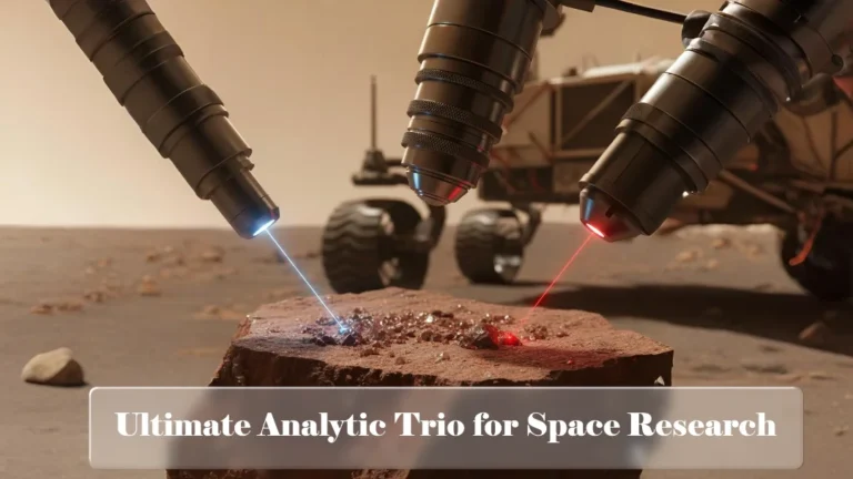
- Sometimes, the best solution is to use multiple analytical techniques together. Just as XRD, SEM, and Raman spectroscopy form a powerful trio in space research, combining AFM and SEM provides a more comprehensive analysis, where SEM gives a broad overview, and AFM zooms in for detailed nanoscale characterization.
AFM guide from Penn State Materials Research Institute | SEM guide from The University of Texas
SEM vs AFM: The Ultimate Showdown on Video
The theoretical comparison is clear, but nothing beats seeing these powerful instruments in action. In this InSciLab Tech video, we settle the debate once and for all with a direct, visual head-to-head comparison.
Inside This Visual Comparison:
We go beyond the specs to show you the real-world performance and data output of each technique.
- 🔍 The Resolution Wars: See the tangible difference between AFM’s atomic-level profiling and SEM’s electron-powered imaging.
- 🧪 Sample Showdown: Watch us analyze conductive metals, soft polymers, and biological samples, demonstrating which technique triumphs for each.
- 📐 3D Imaging Face-Off: Compare AFM’s true 3D topographic maps with SEM’s pseudo-3D depth perception on the same sample.
- ⚡ Speed vs. Detail: Experience the trade-off between SEM’s high-throughput imaging and AFM’s methodical, ultra-detailed scanning.
- 💡 Myth Busting: We put common misconceptions to the test, like “AFM is only for soft materials” and “SEM provides atomic resolution.”
You can read a dozen spec sheets, but seeing the AFM vs SEM data from both machines side-by-side is what truly clarifies the choice.
— The InSciLab Tech Team
Want more deep dives into laboratory technology? Subscribe to InSciLabTech on YouTube for weekly videos that make complex instruments easy to understand.
Conclusion: Making Your Final Choice
The AFM vs SEM comparison reveals a clear, fundamental truth: there is no single “best” microscopy technique, only the best technique for your specific question.
Your decision ultimately boils down to this core trade-off:
- Choose SEM when your priority is speed, large-area imaging, elemental analysis, and investigating rough, conductive, or coated samples.
- Choose AFM when your priority is true 3D topography, atomic-scale resolution, nanomechanical property measurement, and analyzing soft, delicate, or liquid-based samples in their native state.
By using the decision framework in this guide—starting with your sample and your primary research goal—you can confidently select the tool that will deliver the most meaningful data. Remember, these techniques are often complementary; the most powerful insights frequently come from using SEM to identify a region of interest and AFM to probe its nanoscale properties.
As these technologies continue to evolve, pushing the boundaries of resolution and application, your understanding of their core strengths ensures you’ll always choose wisely.
Frequently Asked Questions (FAQ): AFM vs SEM
Can AFM achieve higher resolution than SEM?
Yes, in terms of vertical resolution, AFM is superior, capable of sub-angstrom measurements on flat surfaces. For lateral resolution, high-end SEM can achieve ~1 nm, while AFM can achieve atomic resolution on periodic, flat surfaces. However, AFM’s practical resolution on rough samples can be lower than SEM’s.
Which technique is better for biological samples: AFM or SEM?
AFM is generally preferred for most biological applications. It can image samples in their native, hydrated state (in liquid) without requiring conductive coatings that can alter or damage delicate structures. While SEM can provide high-resolution images of fixed, dried, and coated biological samples, the extensive preparation alters the sample’s natural state.
Do I always need to coat my sample for SEM?
Only non-conductive samples require coating to prevent charging effects that distort the image. Conductive materials like metals typically do not need coating. Non-conductive samples (polymers, ceramics, biological specimens) must be sputter-coated with a thin layer of gold, platinum, or carbon to make them conductive.
Can AFM measure elemental composition like SEM with EDS?
No, AFM cannot perform elemental analysis. It measures surface topography and mechanical properties. If you need elemental composition data, SEM with EDS is the necessary technique. Some researchers use both techniques—first SEM/EDS for elemental mapping, then AFM for 3D topography and mechanical properties.
Which technique has a larger maximum scan size?
SEM has a significantly larger maximum scan size (up to several centimeters), making it ideal for surveying large areas and locating specific features. AFM’s scan size is typically limited to about 100×100 µm, making it suitable for detailed nanoscale analysis of specific regions.
Is AFM really non-destructive to samples?
While AFM is generally considered low-impact, it can potentially damage very soft or fragile samples, especially when operating in contact mode. For delicate materials, tapping mode or other dynamic modes are used to minimize sample damage while still providing high-resolution data.
How much does each instrument cost?
Entry-level AFM systems typically start around $50,000-$100,000, while research-grade SEM systems usually start around $100,000-$200,000. Operational costs for SEM are generally higher due to vacuum system maintenance and required infrastructure.

One Comment